Disclaimer
All circuits documented here are simulation-only designs — no physical fabrication or silicon verification has been performed. Results are based on Cadence Spectre and NGSpice simulations using real foundry BSIM4 PTM 65nm models.
These documents are shared for portfolio and demonstration purposes only and are not intended as educational or reference material. Use in any production or critical application without independent verification is strongly discouraged.
The documentation is Licensed under CC BY 4.0, while the QUCS-S Schematics are Licensed under MIT License. Read the LICENSE.txt in each of these repositories for more information.
General Bias Circuit
Introduction
I have documented only the design procedure, and anything relevant to that. For theory of operation, please refer to standard textbooks or any lectures.
Before we proceed, let's take a look at the schematic of General-bias circuit.


Figure-01: General bias circuit schematic diagram [Ref. CMOS Circuit Design, Layout and Simulation, Fig 20.47]
The upper half is the Beta Multiplier Reference and it's design is already covered seperately in it's own page. The lower half uses BMR to generate wide swing cascode current sink/sources and bias voltages for class-AB output stage.
For designing this, we need to choose values for two things:
- MOSFET Sizes for Cascode bias Voltage generation
- MOSFET Sizes for class-AB bias voltage generation
Since we have already designed the BMR for 10 µA, the general bias circuit will also generate bias voltages for 10 µA. For different current, we have to redesign the BMR as simply using a different size for a specific current will result in mismatch.
Quote
It is strongly recommended that analog designers use only a small set of “unit-sized” transistors, forming all transistors from parallel combinations of these elementary devices.
- Ref. Analog Integrated Circuit design: Tony Chan Caruson, David A. Johns and Kenneth W. Martin, Pg 51
Sizing Cascode Bias Voltage Generation MOSFET
Unlike general design procedure, we will not choose any specific VGS and then find W/L. Instead we will size this MOSFET while keeping a considerable margin in the design space.
Info
That is, we will choose a MOSFET that is smaller than 1/5th of our standard size. This number 1/5 is found using square law equation and solving for this topology (actually it is 1/4th, but that will bias M1 and M2 in Figure-02 at the edge of saturation. 1/5th will bias at slightly into saturation.)


Figure-02: Wide Swing Cascode bias generation from BMR. [Ref. CMOS Circuit Design, Layout and Simulation, Fig 20.38]
Clearly short channel MOSFETs don't follow square law, and hence, in order to design it with ease, we will choose a MOSFET that is even smaller than ⅕th of our standard size, and by this we have made some margin for errors.
Why smaller sizes for cascode generation MOSFET?
Notice that MWS in Figure-02 is also receiving the same current of 10 µA, and when we reduce the size of that MOSFET, the voltage across it will increase. It makes sense as smaller size for the same current should drop a larger voltage across it.
And as this voltage increases, we are increasing VDS of M1 and M2, which will bias it into saturation. After all,
found easily using KVL from Figure-02.
Wouldn't a random size affect bias voltage for M1 and M2?
No it won't, and that's the beauty of Wide Swing Cascode topology. In Figure-02, notice that M1 and M2 are regenerating a new VGS and are not using the VGS generated in BMR.
So, when MWS is changed (smaller than 1/5th of standard size), it will adjust the VGS of both M1 and M2 to make it capable of sinking 10 µA, which can be easily confirmed in Figure-03.

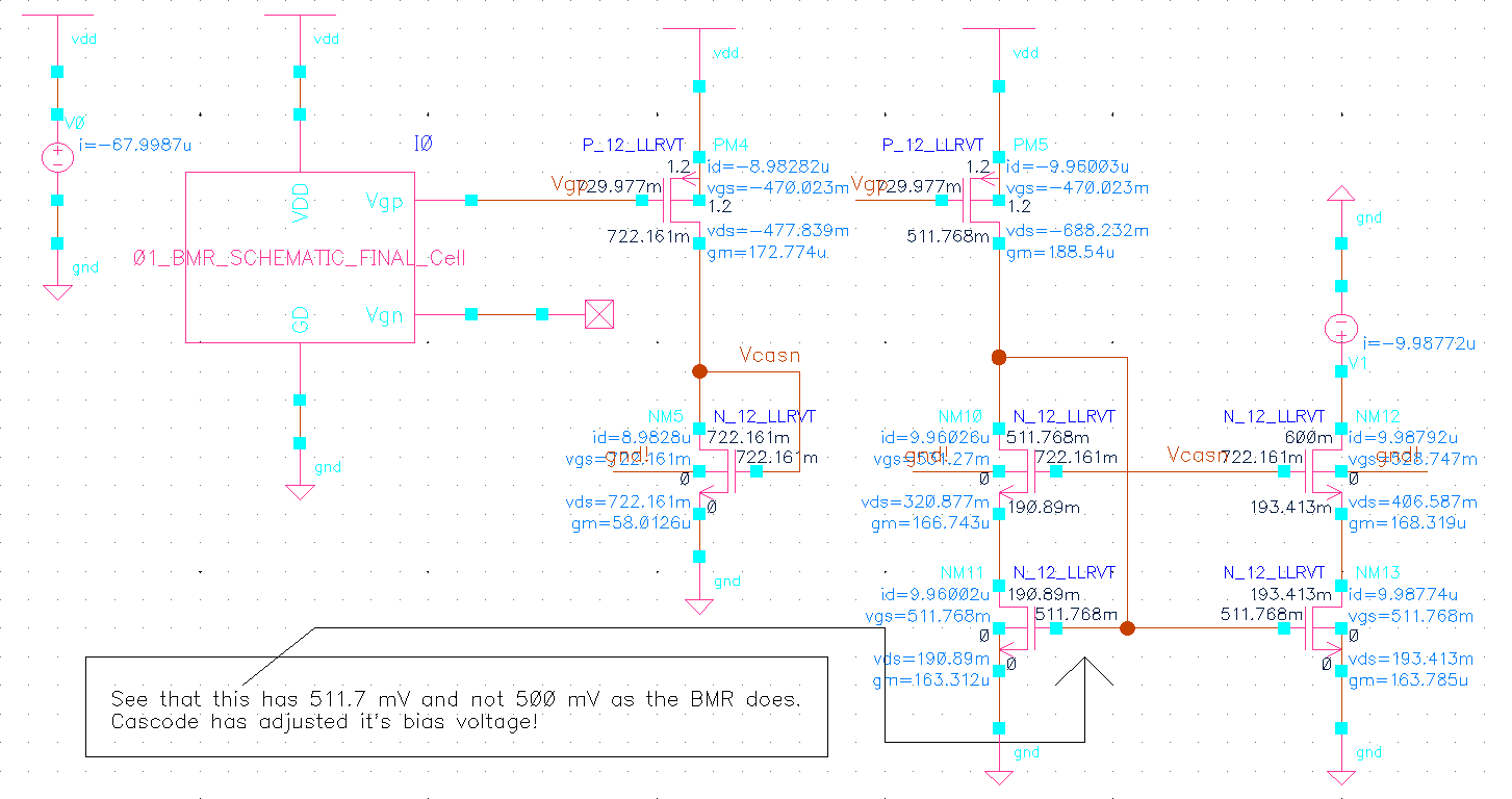
Figure-03: Cascode generation MOSFET size auto adjusts VGS of bottom transistors to sink 10 µA.
It should be noted that our new VGS is not 500 mV as tabulated in Regular Threshold Voltage table, but is changed to 511.7 mV just as expected. And this is not a problem as we will see later.
Danger
This auto adjustment is true as long as the size is small enough. Use a size larger than 1/5th and the output characteristics may turn worse. Keep it sufficiently small.
Trade-off: Smaller Size and Output Characteristics
Output Impedance
From Equation-01, we can see that smaller MWS increases VDS of M1 and M2. When VDS increases, rout increases as seen in Figure-04.


Figure-04: Rout vs VDS of a 43.1/2 NMOS.
And we know that when bottom transistor's output impedance increases, so does the overall cascode's output impedance. But this comes at a price.
Minimum Output Voltage (Minimum compliance Voltage)
Physically, we are increasing VDS of M1 and M2, and that also requires a larger minimum voltage for cascode.
So, the trade-off can be summarised as follows:


Figure-05: Trade-offs summary for Cascode Bias voltage generation MOSFET
Choosing Size for Cascode generation MOSFET
With all the above considerations in mind, you can choose MWS Size 1/10, 1/15, 1/20, and even 1/25 of standard size.
Start from smallest and see what minimum voltage you get, and if it is acceptable, fix it. It's that simple. And it gives the largest output impdedance possible.
Cascode performance for 1/25th of standard size
Let's build Figure-02 with MWS size as 1/25 and also include PMOS Cascode branches from Figure-01. PMOS MOSFET is also chosen to have 1/25 of standard PMOS Sizes.

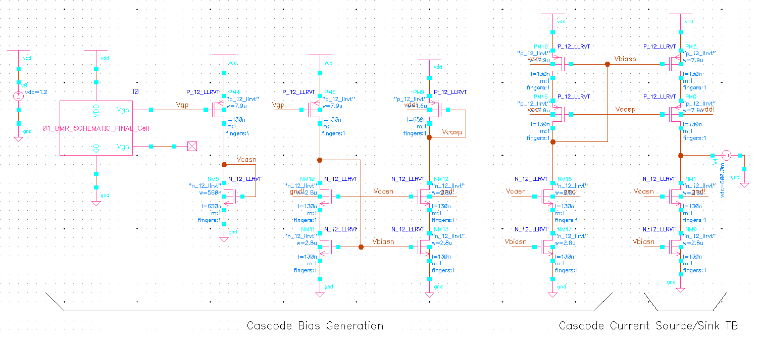
Figure-06: Cascode Current Source/Sink bias generation Test Bench
Here, we will sweep the voltage source V4 from GND to VDD in order to see the output currents of both PMOS Cascode current source and NMOS Cascode current sink.


Figure-07: Cascode Current (a) NMOS Current Sink (b) PMOS Current Source output
From Figure-07 we can see that the minimum voltage needed for both NMOS and PMOS Current Source is roughly 200 mV. For NMOS this is obvious, as it rougly reaches 10 µA around 0.2 V and for PMOS it reaches for less than 1.0 V (i.e., a minimum voltage of \(V_{min} = V_{DD} - V{out,min} = 1.2 - 1.0 = 0.2 V\)).
This is acceptable for me. If you need more minimum voltage, increase size of MWS and reiterate design.
And as such, I am tabulating the cascode generation MOSFET sizes for convenience:
| Flavour | Ratio with standard size | W/L (Drawn) | W/L (Actual) |
|---|---|---|---|
| NMOS | 1/25 | 8.6 / 10 | 560 nm / 650 nm |
| NMOS | 1/25 | 24.6 / 10 | 1.6 µm / 650 nm |
Table-01: Cascode MOSFET sizes summary
It is good to tabulate the output characteristics of this current source (From this point, current source means cascode current source/sink and is shortened for ease of typing.), but I will do it in the conclusion section for ease of reference.
Sizing Class AB Bias Voltage Generation MOSFET
There is no need to size Class AB Bias voltage generation MOSFET and we can just use the standard sizes tabulated in Regular Threshold Voltage to build Figure-01.
Atleast that's how it's supposed to be, but there is a HUGE PROBLEM in this approach.
Insufficient supply for class AB Bias Generation
Yes, you heard it right, there is insufficient supply voltage for class AB bias generation.


Figure-08: Bias Leg for generating PMOS Class AB Bias voltage
See the PMOS case in Figure-08. Clearly, in order to generate the necessary bias voltage, you need 2 * VSG of PMOS. From Figure-01, we can quickly say the same for NMOS case as well.
I will repeat VGS and VSG of our standard sizes here from Regular Threshold Voltage for convenience.
| Flavour | VGSN / VSGP |
|---|---|
| NMOS | 500 mV |
| PMOS | 470 mV |
Table-02: VGS and VSG of Regular Threshold Voltage NMOS and PMOS for our standard sizes.
Let's put some numbers:
That leaves just 0.2 V for our current source. Fortunately, our current source needs just about 0.2 V for proper operation.
Danger
But unfortunately, we're being too optimistic by ignoring BODY EFFECT. That is, PM3 from Figure-08 suffers heavily from body effect. Source of PM3 is away from supply by almost half VDD (As VSG = 0.47 V almost half of VDD = 0.6 V). And that increases our VSG of said PMOS and that means our current source will not get 0.2 V but will get something lesser than that.
This is not good.
Using LVT MOSFET to realise the bias leg under 1.2 V
Now we have two possible course of actions:
- Increase MWS to reduce minimum voltage for current source (at the cost of reduced Rout).
- Or, pick Lower Threshold MOSFET (LVT) instead of Regular Threshold MOSFET (RVT).
I am going to pick LVT, as the current source built using short channel is already plagued with low Rout. I don't want to reduce that, when we have another viable option.
LVT MOSFETs are already sized and tabulated in Low Threshold Voltage and for the sake of convenience the sizes are listed here:
| Flavour | W/L (Drawn) | W/L (Actual) | ID | VGS |
|---|---|---|---|---|
| NMOS | 38.5 / 2 | 2.5 µm / 130 nm | 10 µA | 420 mV |
| PMOS | 93.8 / 2 | 6.1 µm / 130 nm | 10 µA | 420 mV |
Table-03: LVT Sizes and Bias Current summary
Note
Even usage of LVT barely let's us realise a class AB bias leg as VGS without body effect is 420 mV. But even with body effect, this wouldn't eat up the current source's minimum voltage unlike RVT MOSFET.
The drawback is there is a heavy supply dependance, and full 1.2 V is needed for proper operation. So, we're left with a trade-off, where we can get Class AB output stage capable of driving low impedance loads with almost rail-to-rail range (since this class AB uses a CS configuration) but with full supply voltage.
Info
This doesn't mean that the output stage will cease to function at the slightest dip of supply. Only when the supply were to consistently remain at a lower level after a dip (like a battery, which gets constantly discharged as long as it is used) then our output stage will get biased with a lower current (and the pole with that node has moved to lower frequency and may eat up our phase margin. Not good). This means, that the class AB output stage's presence warrants a linear regulator (LDO) at the supply.
DC Simulations
Supply dependance of various bias legs
Now that our sizes are fixed (See Regular Threshold Voltage, Table-01, Table-03) let's build the General bias circuit and see the supply dependance.

Figure-09: Schematic Diagram of General bias circuit (BMR not shown).


Figure-10: Branch currents in (a) BMR, (b) Cascode bias leg, (c) NMOS and PMOS Bias leg and (d) Class AB Bias leg
Some observations:
- Current in NMOS cascode bias leg (Figure-10-b) is slightly less because it is sourced by a simple PMOS current source from BMR and not a cascoded current source (See Figure-02).
- The cascoded current sources (both NMOS sink and PMOS source) show good supply independance and can work with supply voltages as low as 0.7 V (Figure-10-c).
- Current in class AB Bias leg shows heavy supply dependance just as we discussed. It can go as low as 1.0 V with a 20% reduction from target current value (Figure-10-d).
Biasing a Class AB output stage

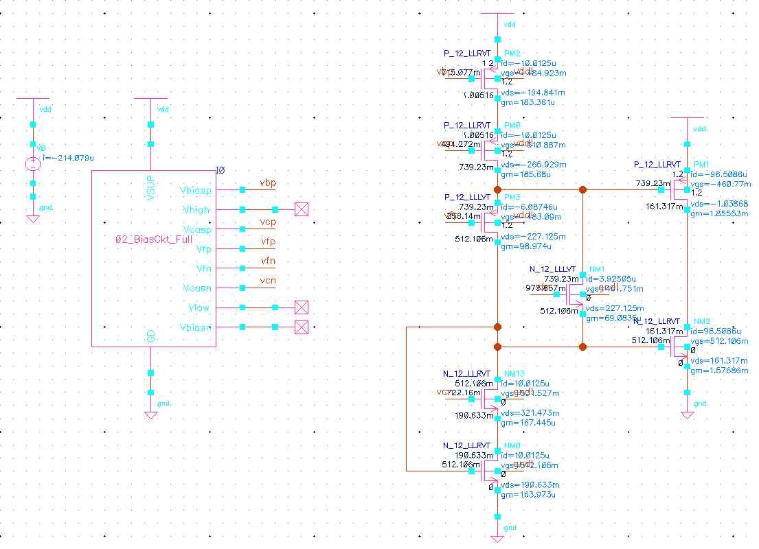
Figure-11: Class AB output stage bias Test bench
Danger
Notice how NMOS NM0 (bottom reference NMOS) is in a diode connected configuration. This is because, you can't put two current sources in series. When you do put two current sources in series, both will duel each other to dictate the current in that branch, and so both will be swinging back and forth between triode and saturation. In order to ease that, I made Current sink derive it's bias voltage as dictated by Current source in order to exactly sink it.
The output MOSFETs have 10 times the width of standard sizes and so are expected to have a current of 100 µA (which they have something very close to 98.5 µA).
Note
The LVT MOSFETs (aka Floating Current sources) used here are half the sizes listed in Table-03, because the total current available in the 1rst branch is just 10 µA and each of them are sized to source/sink that. So, for them to divide it equally between themselves, their sizes are halved. This should not be done as it introduces matching issues. Some ways to mitigate this are:
- Add fingers to reference LVT MOSFETs to help match it to this half sized MOSFET.
- Simply use 2 half-sized MOSFETs in place of reference LVT MOSFETs.
- Add two LVT MOSFETs in series (effectively increasing their length to twice) to help it to source/sink half their sized currents.
I will not do any such iterations to redesign as this documentation is written for demonstration purposes. But, this must be kept in mind when this is designed in a production environment.
Warning
Do not attempt to size these LVT MOSFETs (aka Floating Current sources) to precisely split the 10 µA into two 5 µA branch currents. Even though in Figure-11, the Output stage NMOS is in triode, it's alright as you can and only need to roughly set the VGS for proper biasing. That NMOS is in triode because of keeping two current sources in series (both PMOS and NMOS), and we already discussed what happens when we do so. When signal is applied through a gain stage, that is more than enough to move the VGS of the output MOSFETs to drive load.
Again, Do not attempt for precision design. This precise design methodology is just an illusion spread among the community and do not fall for it!
Transient Simulation - startup action
The BMR possess startup circuit, and it's design is covered in detail in Startup Circuit Design section. You may refer to that.
In order to simulate a circuit powering ON, I applied a voltage step to the supply at 10 ns with a rise time of 20 ns to reach VDD (1.2 V) at 30 ns.


Figure-12: Transient Branch currents in (a) BMR, (b) Cascode bias leg, (c) NMOS and PMOS Bias leg and (d) Class AB Bias leg
Nothing new to observe here other than the fact that the circuit do startup properly and takes about 90 ns to become operational.
Conclusion
The design of General bias circuit is complete.
And for future references, the cascode current source's output characteristics are tabulated here:
| PARAMETER | NMOS SINK | PMOS SOURCE | COMMENTS |
|---|---|---|---|
| Rout | 3.48 MΩ | 5.19 MΩ | Subject to Operating Point |
| Vout,min | 200 mV | 200 mV | Approx. |
| Cascode Bias Generation MOSFET Size to original MOSFET | 1 / 25 | 1 / 25 | Chosen to increase Rout |
Table-04: Cascode Current Source output characteristics summary.